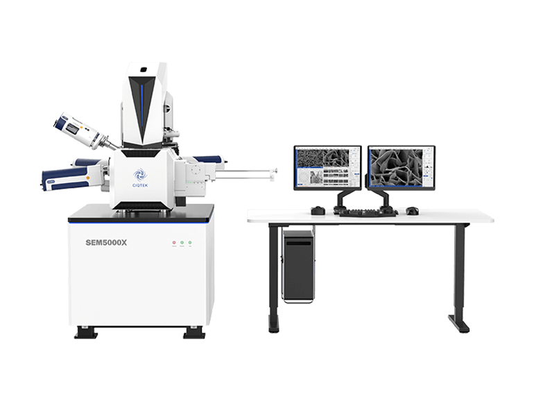
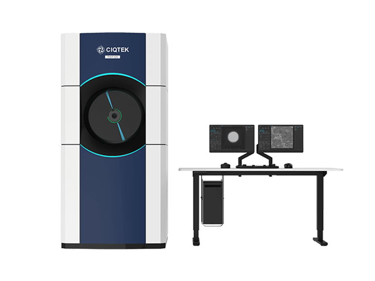
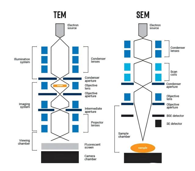
The differences between Scanning Electron Microscope(SEM )and Transmission Electron Microscope(TEM)
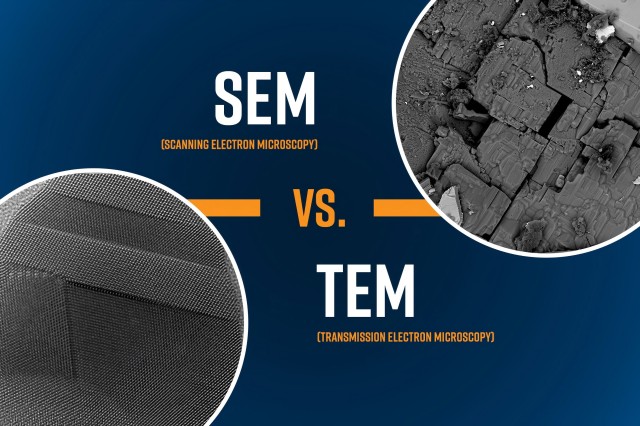
Humans rely on their senses to perceive the world, and these microscopic analysis instruments extend human perception. We are all familiar with optical microscopes, but these microscopes, which work based on lens imaging, are limited by the Abbe limit, where the resolution is limited to half the wavelength of the light used. Therefore, the resolution of optical microscopes is only at the micrometer level due to the limitation of the wavelength of light. However, fast-moving electrons have wave-particle duality, and as a wave, an important characteristic of electrons is their wavelength. With increasing acceleration voltage, the electron wavelength decreases. By using higher acceleration voltages, such as 30 kV, it is possible to obtain electrons with a wavelength of approximately 7 pm. Electron microscopes are created by using electrons as the "light" and substituting magnetic lenses for conventional optical lenses. When electrons interact with a solid specimen, they produce a series of specimen-related information, including induced electromotive force, cathodoluminescence, characteristic X-rays, back-scattered electrons, Auger electrons, secondary electrons, absorbed electrons, transmitted electrons, etc. By utilizing this information, it is possible to obtain structural information at the microscopic scale. The differences between SEM and TEM Source Image from Nanoscience Instrument SEM (Scanning Electron Microscope) and TEM (Transmission Electron Microscope) are two common forms of electron microscopes. SEM uses Secondary Electrons (SE) and Back-scattered Electrons (BSE) to capture images of the specimen surface, while TEM detects transmitted electrons to generate projection images through the specimen's interior. SEM scans the specimen surface with a focused electron beam and collects the signals generated at each point to construct an amplified image pixel by pixel. The scanning coil located below the objective lens guides the beam precisely through the specimen's surface in the X-Y plane. Depending on the magnification (up to 2 million times), the beam scans a field of view ranging from a few micrometers to millimeters. Typical acceleration voltages for SEM range from 1 kV to 30 kV. Lower acceleration voltages provide a gentler beam, which is useful for imaging beam-sensitive and insulating specimens. Secondary electrons are less sensitive to atomic numbers and more suitable for observing surface topography. In contrast, backscattered electrons yield higher signals for specimens with larger atomic numbers, making them suitable for compositional imaging. TEM typically operates at acceleration voltages between 30 kV and 300 kV, which is much higher than the voltages used in SEM instruments, allowing for higher-resolution images. Corrected aberration TEMs can achieve spatial resolutions below 1Å, enabling the observation of very fine details...


