what are you looking for?
Popular Searches
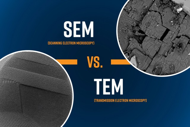
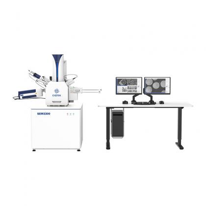
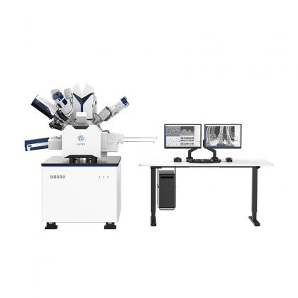
- Field Emission Scanning Electron Microscope manufacturer global supplier
- SEM EDX, EDS, EBSD, BSE, CL, STEM detectors
- scanning nv magnetometer applications
- scanning nv center microscope
- scanning nv magnetometry supplier
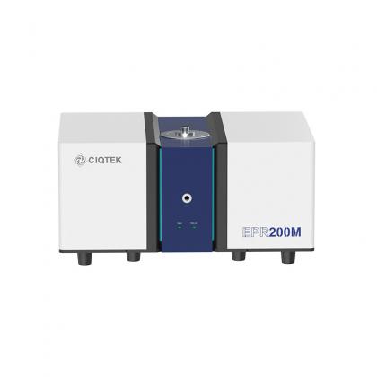
- x band electron paramagnetic resonance spectroscopy
- electron paramagnetic resonance spectroscopy
- epr spectroscopy with cryostat
- w band epr spectrometer
- epr technology