Products
Products
CIQTEK is the manufacturer and global supplier of high-value scientific instruments, such as Scanning Electron Microscopes (SEM and FIB-SEM), Electron Paramagnetic Resonance (Electron Spin Resonance) Spectroscopy, Scanning NV Probe Microscope, Gas Adsorption Analyzer, etc.
scanning electron microscope machine

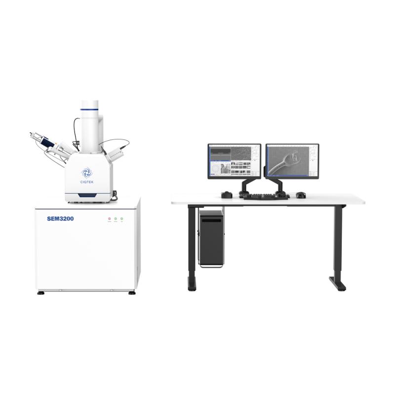
Tungsten Filament SEM | SEM3200

High-performance tungsten filament SEM microscope with excellent imaging quality capabilities in both high and low vacuum modes


The CIQTEK SEM3200 SEM Microscope has a large depth of field with a user-friendly interface to enable users to characterize specimens and explore the world of microscopic imaging and analysis.

  • # Mixing Image (SE+BSE)
    Observe the specimen compositional and surface topographic information in one image
  • # Dual Anode (Tetrode)
    Dual anode emission system design provides excellent resolution under low landing energy
  • # *Low Vacuum Mode
    Provide specimen surface morphology information in low vacuum, switchable vacuum state with one click

(*Optional accessories for SEM Microscope SEM3200)


SEM Detectors for SEM3200

The SEM Microscope is used not only to observe surface morphology but also to analyze the composition of micro-regions on the specimen surface.
CIQTEK SEM Microscope SEM3200 has a large specimen chamber with an extensive interface. In addition to supporting conventional Everhart–Thornley detector (ETD), Backscattered-Electron detector (BSE), and Energy-dispersive X-ray spectroscopy (EDS/EDX), various interfaces such as Electron Backscatter Diffraction Pattern (EBSD) and Cathodoluminescence (CL) are also reserved.
 

>> SEM Backscattered-Electron Detector (BSE)

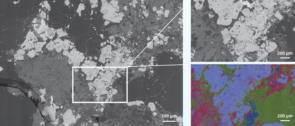
Comparison of secondary electron imaging and backscattered electron imaging

In the backscattered electron imaging mode, the charge effect is significantly suppressed and more information on the composition of the specimen surface can be observed.


Plating Specimens:

  • SEM Backscattered-Electron Detector (BSE) Plating Specimens
  • SEM Backscattered-Electron Detector (BSE) Plating Specimens


Tungsten Steel Alloy Specimens:

  • SEM Backscattered-Electron Detector (BSE) Tungsten Steel Alloy Specimens
  • SEM Backscattered-Electron Detector (BSE) Tungsten Steel Alloy Specimens


Four-quadrants Backscattered Electron Detector - Multi-channel Imaging

The SEM Microscope detector has a compact design and high sensitivity. With the 4-quadrants design, it is possible to obtain topographic images in different directions as well as composition distribution images without tilting the specimen.


Energy Spectrum

LED small bead energy spectrum analysis results.


SEM Energy Spectrum


>> SEM Electron Backscatter Diffraction Pattern (EBSD)

The SEM Microscope SEM3200 with a large beam current fully meets the testing requirements of high-resolution EBSD and can analyze polycrystalline materials such as metals, ceramics, and minerals for crystal orientation and grain size analysis.

The figure shows the EBSD grain map of Ni metal specimen, which can identify grain size and orientation, determine grain boundaries and twins, and make accurate assessments of material organization and structure.


SEM Electron Backscatter Diffraction Pattern (EBSD)


SEM Microscope Models SEM3200A SEM3200
Electro-Optical Systems Electron Gun Pre-aligned Medium-sized Hairpin-type Tungsten Filament
Resolution High Vaccum 3 nm @ 30 kV (SE)
4 nm @ 30 kV (BSE)
8 nm @ 3 kV (SE)
*Low Vaccum 3 nm @ 30 kV (SE)
Magnification 1-300,000x (Film)
1-1000,000x
Acceleration Voltage 0.2 kV ~ 30 kV
Probe Current ≥1.2μA, Real-time display
Imaging Systems SEM Detectors Everhart-Thornley Detector (ETD)
*Backscattered electron detector (BSED), *Low vacuum secondary electron detector(SE), *Energy dispersive spectroscopy (EDS/EDX), etc.
Image Format TIFF, JPG, BMP, PNG
Vacuum System Vacuum Model High Vacuum Better than 5×10⁻⁴ Pa
Low Vacuum 5 ~ 1000 Pa
Control Mode Fully Automated Control
Specimen Chamber Camera Optical Navigation
Monitoring in the Specimen Chamber
Specimen Table Three Axis Automatic Five Axis Automatic
Stage Range X: 120 mm X: 120 mm
Y: 115 mm Y: 115 mm
Z: 50 mm Z: 50 mm
/ R: 360°
/ T: -10° ~ +90°
Software Operating System Windows
Navigations Optical Navigation, Gesture Quick Navigation
Automatic Functions Auto Brightness & Contrast, Auto Focus, Automatic Stigmator
Special Functions

Intelligence Assisted Image Astigmatism Correction

*Large-FOV Image Stitching (Optional) 

Installation Requirements Temperature 20°C (68°F) ~ 25°C (77°F)
Humidity ≤ 50 %
Power Supply

AC 220 V (±10 %), 50 Hz, 2 kVA

AC 110V (±10%), 60Hz


CIQTEK SEM Microscope SEM3200 Technique Highlights


> Low Voltage SEM

Carbon material specimens with shallow penetration depth at the low voltage. The true topography of the specimen surface can be obtained with rich details.


The electron beam irradiation damage of the hair specimen is reduced at low voltage while the charge effect is eliminated.


Low Vacuum SEM

Filtered fiber tube materials are poorly conductive and charge significantly in high vacuum. Direct observation of non-conductive specimens can be done in a low vacuum without coating by SEM Microscope SEM3200.


Large Field of View

Biological specimens, using a large field of view observation, can easily obtain the overall morphology details of a ladybug's head, demonstrating cross-scale imaging ability.

  • SEM Large Field of View
  • SEM Large Field of View


Specimen Stage Navigation & Anti-collision

Optical Navigation

Click where you want to go and see with easy navigation when using CIQTEK SEM Microscopes.

An in-chamber camera is standard and can take HD photos to help locate specimens quickly.

  • SEM Microscope Specimen Stage Navigation & Anti-collision


Quick Gesture Navigation

CIQTEK SEM Microscope SEM3200 Quick navigation is achieved by double-clicking to move, using the middle mouse button to drag, and using the frame to zoom.

Exp: Frame Zoom - to get a large view of the specimen with low magnification navigation, you can quickly frame the specimen area you are interested in, image zooms in automatically to improve efficiency.

  • SEM Microscope Quick Gesture Navigation
  • SEM Microscope Quick Gesture Navigation


Stage Anti-collision

CIQTEK SEM Microscope SEM3200 Multi-way Anti-collision Solutions:

1. Manually input specimen height: precisely control the distance between the specimen surface and the objective lens.

2. Image recognition and motion capture: monitor the real-time stage movement.

3. *Hardware: shut down the stage motor at the moment of collision.

  • SEM Microscope Stage Anti-collision


Characteristic Functions

Intelligence Assisted Image Astigmatism Correction

Visually display astigmatism within the entire field of view, and quickly adjust to correct by mouse clicking.

  • SEM Microscope Intelligence Assisted Image Astigmatism Correction
  • SEM Microscope Intelligence Assisted Image Astigmatism Correction


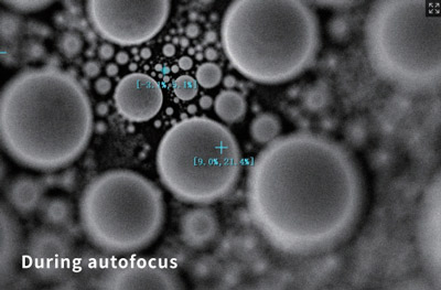
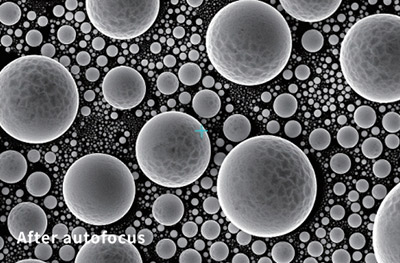
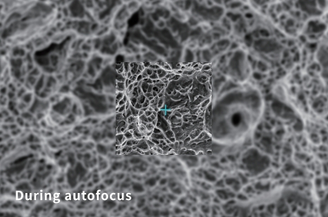
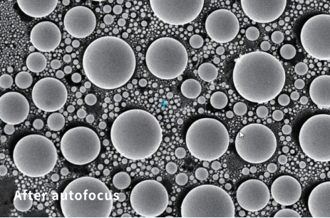
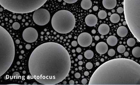
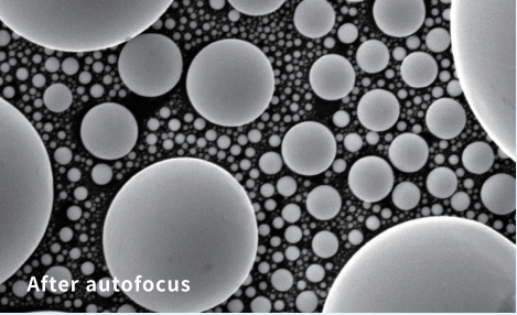
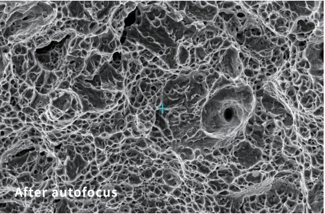
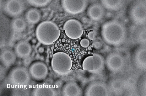
Auto-focus SEM

One-button focus for fast imaging.

  • SEM Microscope Auto Focus
  • SEM Microscope Auto Focus


Automatic Stigmator

One-click astigmatism deduction to improve work efficiency.

  • SEM Microscope Automatic Stigmator
  • SEM Microscope Automatic Stigmator


Auto Brightness & Contrast

One-click auto brightness & contrast to tune appropriate images' grayscale.

  • SEM Microscope Auto Brightness & Contrast
  • SEM Microscope Auto Brightness & Contrast


Simultaneous Imaging of Multiple Information

The CIQTEK SEM Microscope SEM3200 software supports one-click switching between SE and BSE for mixed imaging. Both morphological and compositional information of the specimen can be observed at the same time.

SEM Microscope Simultaneous Imaging of Multiple Information


Fast Image Rotation Adjustment

Drag a line and release to rotate the image right on the spot.

  • SEM Microscope Fast Image Rotation Adjustment
  • SEM Microscope Fast Image Rotation Adjustment
  •  


Leave A Message
Please feel free to contact us for more details, request a quote or book an online demo! We will reply you as soon as we can.
Submit
Related Products
fib sem microscopy

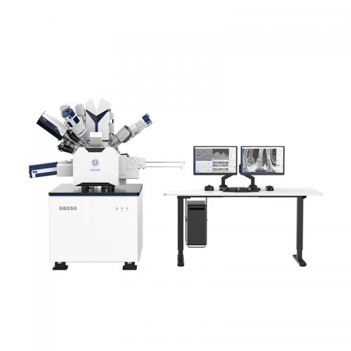
Field Emission Scanning Electron Microscope (FE-SEM) with Focused Ion Beam (FIB) Columns   The CIQTEK DB500 Focused Ion Beam Scanning Electron Microscope (FIB-SEM) adopts “SuperTunnel” electron optics technology, low aberration, and non-magnetic objective design with low voltage and high-resolution capability to ensure the nano-scale analysis. The ion column facilitates a Ga+ liquid metal ion source with a highly stable and high-quality ion beam for nanofabrication.   FIB-SEM DB500 has an integrated nano-manipulator, gas injection system, electrical anti-contamination mechanism for the objective lens, and 24 expansion ports, making it an all-around nano-analysis and fabrication platform with comprehensive configurations and expandability.

Learn More
fesem edx

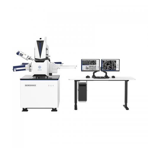
Ultra-high resolution Field Emission Scanning Electron Microscopy (FESEM): 0.6 nm@15 kV and 1.0 nm@1 kV   The CIQTEK SEM5000X ultra-high resolution FESEM utilizes the upgraded column engineering process, “SuperTunnel” technology, and high-resolution objective lens design to improve low-voltage imaging resolution. The FESEM SEM5000X specimen chamber ports extend to 16, and the specimen exchange load-lock supports up to 8-inch wafer size (maximum diameter 208 mm), significantly expanding the applications. The advanced scanning modes and enhanced automated functions bring stronger performance and an even more optimized experience.

Learn More
field emission scanning electron microscope fe sem

Analytical field emission scanning electron microscope (FESEM) equipped with a high-brightness long-life Schottky field emission electron gun   With the three-stage condenser electron optics column design for beam currents up to 200 nA, SEM4000Pro delivers advantages in EDS, EBSD, WDS, and other analytical applications. The system supports low vacuum mode as well as a high-performance low-vacuum secondary electron detector and retractable backscattered electron detector, which can help directly observe poorly conductive or even non-conductive samples. Standard optical navigation mode and an intuitive user operation interface make your analysis work easy.

Learn More
field emission scanning electron microscopy

CIQTEK SEM5000Pro is a field emission scanning electron microscope (FESEM) with high-resolution imaging and analysis ability, supported by abundant functions, benefits from advanced electron optics column design, with high-pressure electron beam tunnel technology (SuperTunnel), low aberration, and MFL objective lens, achieves low voltage high-resolution imaging, the magnetic specimen can also be analyzed. With optical navigation, automated functionalities, carefully designed human-computer interaction user interface, and optimized operation and use process, no matter if you are an expert or not, you can quickly get started and complete high-resolution imaging and analysis work.

Learn More
sem electron microscope

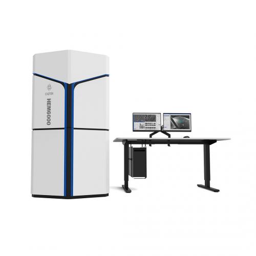
High-speed scanning electron microscope for cross-scale imaging of large-volume specimens   CIQTEK HEM6000 facilities technologies such as the high-brightness large-beam current electron gun, high-speed electron beam deflection system, high-voltage sample stage deceleration, dynamic optical axis, and immersion electromagnetic & electrostatic combo objective lens to achieve high-speed image acquisition whilst ensuring nano-scale resolution. The automated operation process is designed for applications such as a more efficient and smarter large-area high-resolution imaging workflow. The imaging speed can reach more than 5 times faster than a conventional field emission scanning electron microscope (fesem).

Learn More
Top

Leave A Message

Leave A Message
Please feel free to contact us for more details, request a quote or book an online demo! We will reply you as soon as we can.
Submit

Home

Products

Chat

contact