CIQTEK FIB-SEM Practical Demonstration - TEM Sample Preparation
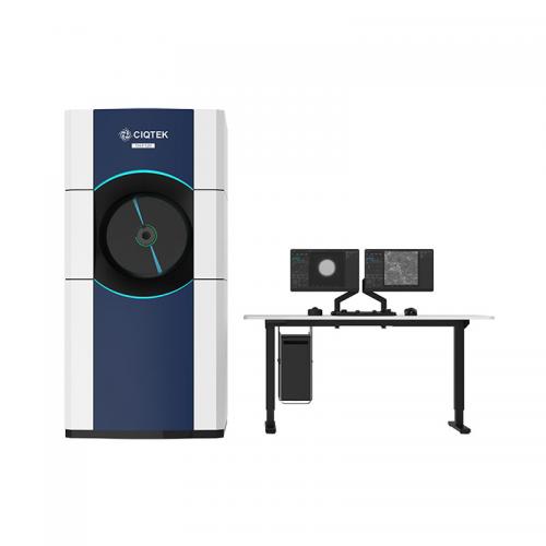
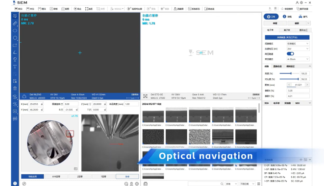
FIB-SEM can be used for defect diagnosis, repair, ion implantation, in-situ processing, mask repair, etching, integrated circuit design modification, chip device production, and mask-less processing of large-scale integrated circuits. Nanostructure production, complex nanopattern processing, three-dimensional imaging and analysis of materials, ultra-sensitive surface analysis, surface modification, and transmission electron microscopy sample preparation, etc. It has a wide range of application requirements and is indispensable. CIQTEK DB500 is a Field Emission Scanning Electron Microscope (FE-SEM) with a Focused Ion Beam (FIB) column for nano analysis and specimen preparation, which is applied with “SuperTunnel” electron optics technology, low aberration, and magnetic-free objective lens design, with low-voltage and high-resolution ability that ensures its nano-scale analytical capability. The ion column facilitates a Ga+ liquid metal ion source with a highly stable and high-quality ion beam to ensure nano-fabrication capability. DB500 has an integrated nano-manipulator, gas injection system, electrical anti-contamination mechanism for the objective lens, and 24 expansion ports, making it an all-around nano-analysis and fabrication platform with comprehensive configurations and expandability. In order to demonstrate the outstanding performance of DB500 to users, the Electron Microscopy team has specially planned the special program " CIQTEK FIB Show", which will present the wide range of applications in the fields of materials science, semiconductor industry, biomedicine, etc. in the form of video. The audience will understand the working principle of DB500, appreciate the stunning microscopic images it captures, and deeply explore the significance of this technology to scientific research and industrial development. TEM sample preparation In this episode, we will show you how DB500 can prepare transmission electron microscope (TEM) samples efficiently and accurately. As you can see from the video, DB500 prepares TEM samples with simple operation, few pre-processing steps, low learning costs, and efficient testing; it can achieve precise micro- and nanoscale cutting at fixed points, with controllable size and uniform thickness, and is suitable for a variety of microscopy and Microscopic spectroscopy analysis; and the integration of cutting, imaging, and analysis can be achieved.


