On July 13, the 11th Analytica China was successfully concluded at the National Convention and Exhibition Center (Shanghai). As a lighthouse exhibition in the laboratory industry, this year's show gathered 1,273 exhibitors and cooperative units, and 56,864 professional visitors to join the grand event.
CIQTEK comprehensively demonstrated its advanced measurement technologies, products, and solutions centered on precision measurement technology at the conference, magnetic resonance, electron microscopy, gas adsorption analysis, and weak-signal measurement series products appearing in full and gaining a lot of attention.
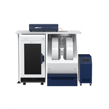
Based on the self-developed Electron Paramagnetic Resonance Spectrometer (EPR) and Gas Adsorption Analyzer, CIQTEK's application experts shared the application of EPR, Specific Surface and Pore Size Analysis technologies in the field of environmental catalysis as well as Gas Adsorption Analysis technologies in the characterization of pharmaceuticals in the booth in the form of offline+online, which provided the solutions of domestically-made high-end scientific instruments for the application research in the related fields and attracted a large number of audiences to visit the booth and exchange ideas.
CIQTEK SEM5000 is a field emission scanning electron microscope(FESEM) with high-resolution imaging and analysis ability, supported by abundant functions, benefits from advanced electron optics column design, with high-pressure electron beam tunnel technology (SuperTunnel), low aberration, and non-immersion objective lens, achieves low voltage high-resolution imaging, the magnetic specimen can also be analyzed. With optical navigation, automated functionalities, carefully designed human-computer interaction user interface, and optimized operation and use process, no matter if you are an expert or not, you can quickly get started and complete high-resolution imaging and analysis work.
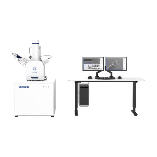
High-performance and Universal Tungsten Filament SEM Microscope The CIQTEK SEM3200 SEM Microscope is an excellent general-purpose Tungsten Filament Scanning Electron Microscope (SEM) with outstanding overall capabilities. Its unique Dual-anode electron gun structure ensures high resolution and improves image signal-to-noise ratio at low excitation voltages. Furthermore, it offers a wide range of optional accessories, making the SEM3200 a versatile analytical instrument with excellent expendabilities.
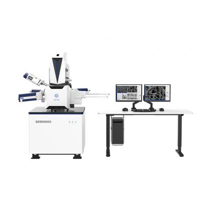
Ultra-high Resolution Field Emission Scanning Electron Microscopy (FESEM) Challenges the Limits The CIQTEK SEM5000X is an ultra-high resolution FESEM with optimized electron optics column design, reducing overall aberrations by 30%, achieving ultra-high resolution of 0.6 nm@15 kV and 1.0 nm@1 kV. Its high resolution and stability make it advantageous in advanced nano-structural materials research, as well as the development and manufacturing of high-technology node semiconductor IC chips.
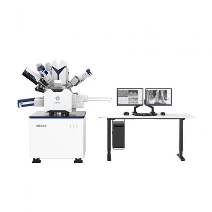
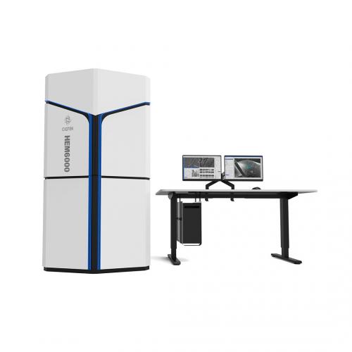
High-speed Scanning Electron Microscope for Cross-scale Imaging of Large-volume Specimens CIQTEK HEM6000 facilities technologies such as the high-brightness large-beam current electron gun, high-speed electron beam deflection system, high-voltage sample stage deceleration, dynamic optical axis, and immersion electromagnetic & electrostatic combo objective lens to achieve high-speed image acquisition whilst ensuring nano-scale resolution. The automated operation process is designed for applications such as a more efficient and smarter large-area high-resolution imaging workflow. The imaging speed can reach over 5 times faster than a conventional field emission scanning electron microscope (FESEM).
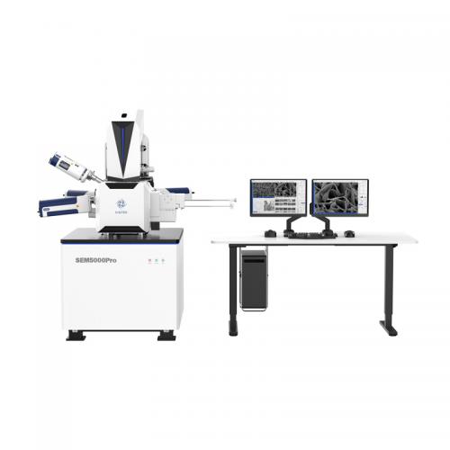
High Resolution under Low Excitation The CIQTEK SEM5000Pro is a Schottky field emission scanning electron microscope (FE-SEM) specialized at high resolution even under low excitation voltage. Employing an advanced "Super-Tunnel" electron optics technology facilitates a crossover-free beam path together with an electrostatic-electromagnetic compound lens design. These advancements reduce spatial charging effect, minimize lens aberrations, enhance imaging resolution at low voltage, and achieve a resolution of 1.2 nm at 1 kV, which allows for direct observation of non-conductive or semi-conductive samples, effectively reducing sample irradiation damage.
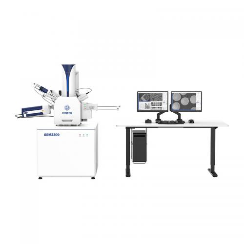
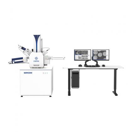
Next-generation Tungsten Filament Scanning Electron Microscope The CIQTEK SEM3300 scanning electron microscope (SEM) incorporates technologies such as "Super-Tunnel" electron optics, inlens electron detectors, and electrostatic & electromagnetic compound objective lens. By applying these technologies to the tungsten filament microscope, the long-standing resolution limit of such SEM is surpassed, enabling the tungsten filament SEM to perform low-voltage analysis tasks previously only achievable with field emission SEMs.
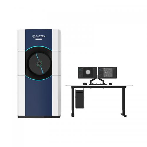
120kV Field Emission Transmission Electron Microscope (TEM) 1. Divided Workspaces: Users operate TEM in a divided room with comfort reducing environmental interference to TEM. 2. High Operational Efficiency: Designated software integrates highly automated processes, allowing efficient TEM interaction with real-time monitoring. 3. Upgraded Operational Experience: Equipped with a field emission electron gun with a highly automated system. 4. High Expandability: There are sufficient interfaces reserved for users to upgrade to a higher configuration, which meets diverse application requirements.